S
I
L
I
C
O
N
I
N
G
O
T
Silicon Ingot Technology has completed an intensive, multi-city research and development tour across several of Asia’s most advanced semiconductor and photovoltaic manufacturing regions. This strategic initiative reflects our continued commitment to learning, innovation, and mastering the world’s most complex crystal growth technologies.
Over the past weeks, our leadership and engineering teams travelled across major RCD hubs in China, visiting factories, universities, exhibitions, conferences, and specialized research laboratories. The purpose of the tour was to further deepen our technical expertise in mono-crystalline and poly-crystalline silicon ingot manufacturing, while exploring global advancements shaping the future of PV and semiconductor materials.
At Silicon Ingot Technology, we believe that true capability comes from continuous learning and direct exposure to global manufacturing excellence. The RCD tour was designed to:
This mission aligns with our vision to build a world-class, high-purity silicon ingot manufacturing ecosystem.
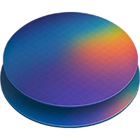
Our teams visited top crystal growth factories specializing in, G6, G8, and G12 ingot production.
These visits provided priceless exposure to the precision required to achieve consistent resistivity, structural perfection, and high-volume ingot stability.
We met with scientists, professors, and material researchers to discuss:
These conversations will help us strengthen our internal RCD and testing capabilities.
At major international events in Shanghai and Jiangsu, we explored:
We also networked with suppliers, machine manufacturers, and global technology partners.
This R&D mission directly enhances the quality of our ingots and future wafer products.
Customers can expect improvements in:
These advancements strengthen our ability to deliver ultra-pure, globally competitive silicon ingots for both solar and semiconductor industries.
At Silicon Ingot Technology, we continuously push ourselves to study, explore, and innovate.
We believe that mastering silicon ingot manufacturing requires dedication far beyond basic operations
Following this R& D tour, we are now:
Our long-term vision is to create a world-class silicon ecosystem combining global expertise with India’s rising manufacturing strength. Stay Connected For more updates, follow our News section or connect with us on LinkedIn and Instagram.
Silicon Ingot Technology will continue sharing insights from our journey as we grow into a leading force in high-purity silicon materials